

-
-
-
Customer Stories 》
-
-


Product center
-
The V8S/V8H Inline Vacuum Soldering Oven features ultra-low vacuum level, high output, low energy consumption, low nitrogen consumption and compact footprint. The V8S/V8H is specially optimized and designed for the specific vacuum soldering and packaging requirements of lead frame products, LED products and power devices in the semiconductor industry. It is a carefully engineered vacuum oven developed to address various challenges encountered by customers in the current industry.Welding Temperature: The maximum actual welding temperature of the VPO300 vacuum positive pressure sintering furnace is ≥800℃. Vacuum Degree: Ultimate vacuum degree ≤5×10⁻² torr. Positive Pressure Capacity: 0.5Mpa (1Mpa optional). Effective Welding Area: ≥300mm×300mm.Soldering Temperature Maximum actual soldering temperature ≤ 600℃ Vacuum Level Ultimate vacuum ≤ 10 Pa; Working vacuum: 50 Pa – 200 Pa Effective Soldering Area ≥ 380 mm × 310 mmSoldering Temperature Maximum actual soldering temperature of the V3DR Formic Acid Reflow Oven ≤ 600℃ Vacuum Level Ultimate vacuum ≤ 0.3 Pa; Working vacuum: 5 Pa – 200 Pa Temperature Uniformity ≤ ±1% within the effective soldering area Effective Soldering Area ≤ 300 mm × 300 mmThe V8S/V8H Inline Vacuum Soldering Oven features ultra-low vacuum level, high output, low energy consumption, low nitrogen consumption and compact footprint. The V8S/V8H is specially optimized and designed for the specific vacuum soldering and packaging requirements of lead frame products, LED products and power devices in the semiconductor industry. It is a carefully engineered vacuum oven developed to address various challenges encountered by customers in the current industry.The V8SL vacuum formic acid reflow oven features ultra-low vacuum degree, high throughput, low energy consumption, low nitrogen consumption and compact footprint. Specifically optimized and designed for the semiconductor industry, the V8SL is a dedicated vacuum oven for vacuum welding and packaging of lead frame products, LED products and power devices, addressing various pain points currently faced by industry customers.Drastically reduces welding bubbles in solder, resulting in a void ratio as low as 1–2%. Enhances the electrical performance of products and the bonding strength of soldered joints, effectively improving the reliability and quality of solder points. Applicable for double-sided PCB soldering, suitable for mass production and continuous production line integration, with an average production cycle controlled at 30–60s.Drastically reduces welding bubbles in solder, resulting in a void ratio as low as 1–2%. Enhances the electrical performance of products and the bonding strength of soldered joints, effectively improving the reliability and quality of solder points. Applicable for double-sided PCB soldering, suitable for mass production and continuous production line integration, with an average production cycle controlled at 30–60s.
-
 Drastically reduces welding bubbles in solder, resulting in a void ratio as low as 1–2%. Enhances the electrical performance of products and the bonding strength of soldered joints, effectively improving the reliability and quality of solder points. Applicable for double-sided PCB soldering, suitable for mass production and continuous production line integration, with an average production cycle controlled at 30–60s.
 Drastically reduces welding bubbles in solder, resulting in a void ratio as low as 1–2%. Enhances the electrical performance of products and the bonding strength of soldered joints, effectively improving the reliability and quality of solder points. Applicable for double-sided PCB soldering, suitable for mass production and continuous production line integration, with an average production cycle controlled at 30–60s.
 The furnace consists of 4 independent process chambers: 2 Preheating Zones, 1 Heating Zone and 1 Cooling Zone; each chamber is fitted with a viewing window, and the pressure of the process chamber ranges from 20 to 200 Pa. The furnace supports and enables precise control of nitrogen, formic acid (nitrogen + formic acid) atmospheres, and is compatible with preformed solder foil processes. Programmable multi-stage vacuum pumping function: Each chamber is equipped with an independent vacuum pump and control system, with a vacuum level ≤ 20 Pa and a pumping speed of 200 m³/h. A soft pumping valve is installed for adjustable pumping rate. The vacuum value of the chamber is displayed in real time and can be controlled and adjusted.
 The furnace consists of 5 zones: Loading Zone, Preheating Zone, Heating Zone, Cooling Zone and Unloading Zone. It is configured with a double-layer vacuum chamber (internal and external), a distinctive design compared with the single-layer vacuum chambers of similar equipment. This double-layer structure ensures zero workpiece oxidation and formic acid leakage prevention, with the oxygen content maintained below 5 ppm.
 The furnace consists of 3 independent process chambers for Preheating, Heating and Cooling respectively; each chamber is fitted with a viewing window, and the pressure of the process chamber ranges from 0.2 to 1050 mbar. The furnace supports and enables precise control of nitrogen, formic acid (nitrogen + formic acid) atmospheres, and is compatible with preformed solder foil processes. Programmable multi-stage vacuum pumping function: Each chamber is equipped with an independent vacuum pump and control system, with a vacuum level ≤ 1 mbar and a pumping speed of 100 m³/h. A soft pumping valve is installed for adjustable pumping rate. The vacuum value of the chamber is displayed in real time and can be controlled and adjusted.
 Drastically reduces welding bubbles in solder, resulting in a void ratio as low as 1–2%. Enhances the electrical performance of products and the bonding strength of soldered joints, effectively improving the reliability and quality of solder points. Applicable for double-sided PCB soldering, suitable for mass production and continuous production line integration, with an average production cycle controlled at 30–60s.
 The furnace consists of 5 zones: Loading Zone, Preheating Zone, Heating Zone, Cooling Zone and Unloading Zone. It is configured with a double-layer vacuum chamber (internal and external), a distinctive design compared with single-layer vacuum chambers of similar equipment. The double-layer structure ensures zero workpiece oxidation and formic acid leakage prevention, with the oxygen content maintained below 5 ppm.
 Inline Formic Acid Vacuum Sintering Furnace — VF680 The furnace consists of 3 independent process chambers for preheating, heating and cooling respectively; each chamber is equipped with a viewing window, and the pressure of the process chamber ranges from 0.2 to 1050 mbar. The furnace supports and enables precise control of nitrogen, formic acid (nitrogen + formic acid) atmospheres, and is compatible with preformed solder foil processes.
 -
 This fully automatic nano silver/nano copper positive pressure sintering furnace is primarily designed for mechanical pressure sintering. For the pressure application unit, a precision hydraulic control system is adopted in this design to achieve high-precision pressure exertion.
 This nano silver positive pressure sintering furnace is primarily based on mechanical pressure curing. For the pressure application unit, a precision hydraulic control system is adopted in this design to achieve high-precision pressure exertion.
 This fully automatic nano silver/nano copper positive pressure sintering furnace is primarily designed for mechanical pressure sintering. For the pressure application unit, a precision hydraulic control system is adopted in this design to achieve high-precision pressure exertion.
 This furnace is mainly for mechanical pressure sintering. For the pressure application unit, a precision pressure control system is adopted in this design to achieve high-precision pressure exertion. A vacuum-sealed structure is applied to the overall furnace chamber and structural design. The sintering process can be carried out in a vacuum environment or two or more types of atmospheres, which improves the product sintering quality.
 Nano Silver Positive Pressure Sintering Furnace — SIN350S This nano silver positive pressure sintering furnace is mainly based on mechanical pressure curing. For the pressure application unit, this design adopts a precision hydraulic control system to achieve high-precision pressure exertion.
 This nano silver positive pressure sintering furnace is primarily based on mechanical pressure curing. For the pressure application unit, this design adopts a precision hydraulic/electric servo control system to achieve high-precision pressure exertion.
 -
 A. Each zone is heated simultaneously from top and bottom for more uniform temperature distribution. B. Advanced formic acid reflow process is adopted to effectively remove oxides and contaminants.
 Soldering Temperature Maximum actual soldering temperature of the high-cleanliness vacuum eutectic furnace ≥ 500℃
 Basic Technical Parameters Soldering Temperature: Maximum actual soldering temperature ≥ 500℃ Vacuum Level: Ultimate vacuum ≤ 10 Pa; Working vacuum 10 Pa Effective Soldering Area: ≥ 260mm×240mm Furnace Chamber Height: ≥ 100mm (customizable for special heights) Temperature Uniformity: ≤ 1% within the effective soldering area Heating Rate: Maximum heating rate of the platform ≤ 120℃/min (controllable) Cooling Rate: Maximum 60-120℃/min (cooling slope for 100℃ drop at no-load maximum temperature, controllable via process)
 The WRO1300 is an inline wafer vacuum formic acid oven characterized by high throughput, low energy consumption, low nitrogen usage, and mobility. It is a vacuum soldering and packaging furnace with 13 temperature-controlled stations, specifically designed for chip soldering processes.
 -
 The N10 is a 10-zone online nitrogen formic acid oven, designed to meet customers' production capacity requirements. With an oxygen content of less than 20 PPM, it is suitable for high-quality packaging and soldering of frame products and CLIP products.
 The N300 is a bench-top offline device suitable for small-batch production, mainly serving laboratories, research institutes and customers with low production capacity requirements.
 The N300A is a bench-top offline device designed for small-batch production. It is mainly suitable for laboratories, research institutes, and customers with low production capacity requirements.
 Computer Control Operate the controller parameters via dedicated software to boost production efficiency, enabling soldering production for a diverse range of products.
 Computer Control Operate controller parameters through software to improve production efficiency, which can meet the soldering production under the condition of product diversification.
Computer Control Operate controller parameters through software to improve production efficiency, which can meet the soldering production under the condition of product diversification.
Computer Control Operate controller parameters through software to improve production efficiency, which can meet the soldering production under the condition of product diversification. -
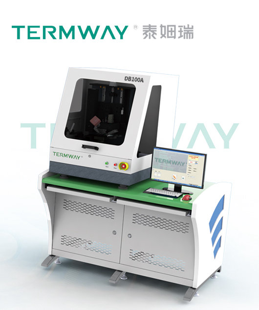
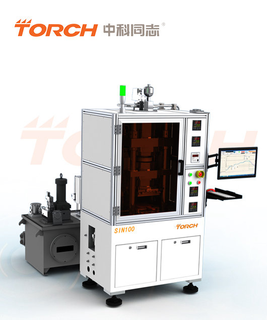
 The DB100A is a manual and semi-automatic silver sintering die bonder. The whole machine adopts a marble motion platform to ensure the overall motion accuracy reaches the submicron level. Equipped with a built-in laser height measurement system, it is suitable for die attach and eutectic soldering of deep cavity substrates. Optional configurations include a nozzle heating module, nozzle pressure feedback system, UV dispensing and curing module, nitrogen protection gas module, substrate preheating module, process monitoring module and chip flip-chip mounting module.
 The DB100A is a manual and semi-automatic silver sintering die bonder. The whole machine adopts a marble motion platform to ensure the overall motion accuracy reaches the submicron level. Equipped with a built-in laser height measurement system, it is suitable for die attach and eutectic soldering of deep cavity substrates. Optional configurations include a nozzle heating module, nozzle pressure feedback system, UV dispensing and curing module, nitrogen protection gas module, substrate preheating module, process monitoring module and chip flip-chip mounting module.
The DB160A is a manual and semi-automatic silver sintering die bonder. The whole machine adopts a marble motion platform to ensure the overall motion accuracy reaches the submicron level. Equipped with a built-in laser height measurement system, it is suitable for die attach and eutectic soldering of deep cavity substrates. Optional configurations include a nozzle heating module, nozzle pressure feedback system, UV dispensing and curing module, nitrogen protection gas module, substrate preheating module, process monitoring module and chip flip-chip mounting module.
The DB100S is a manual-semi-automatic micro-assembly die mounting system. The whole machine adopts a marble motion platform to ensure the overall motion accuracy reaches the submicron level. Equipped with a built-in laser height measurement system, it is suitable for die attach and eutectic soldering of deep cavity substrates. Optional configurations include a nozzle heating module, nozzle pressure feedback system, UV dispensing and curing module, nitrogen protection gas module, substrate preheating module, process monitoring module and chip flip-chip mounting module. The mounting accuracy of the system can reach 1μm with different configurations, and the nozzle can be manually replaced for chips of different sizes. It is an essential equipment for high-precision die attach and bonding in high-end medical devices (core imaging module assembly), optical devices (laser LD bar assembly, VCSEL, PD, LENS assembly, etc.) and semiconductor chips (MEMS devices, RF devices, microwave devices an
The DB100A is a manual and semi-automatic silver sintering die bonder. The whole machine adopts a marble motion platform to ensure the overall motion accuracy reaches the submicron level. Equipped with a built-in laser height measurement system, it is suitable for die attach and eutectic soldering of deep cavity substrates. Optional configurations include a nozzle heating module, nozzle pressure feedback system, UV dispensing and curing module, nitrogen protection gas module, substrate preheating module, process monitoring module and chip flip-chip mounting module.
The DB160A is a manual and semi-automatic silver sintering die bonder. The whole machine adopts a marble motion platform to ensure the overall motion accuracy reaches the submicron level. Equipped with a built-in laser height measurement system, it is suitable for die attach and eutectic soldering of deep cavity substrates. Optional configurations include a nozzle heating module, nozzle pressure feedback system, UV dispensing and curing module, nitrogen protection gas module, substrate preheating module, process monitoring module and chip flip-chip mounting module.
The DB100S is a manual-semi-automatic micro-assembly die mounting system. The whole machine adopts a marble motion platform to ensure the overall motion accuracy reaches the submicron level. Equipped with a built-in laser height measurement system, it is suitable for die attach and eutectic soldering of deep cavity substrates. Optional configurations include a nozzle heating module, nozzle pressure feedback system, UV dispensing and curing module, nitrogen protection gas module, substrate preheating module, process monitoring module and chip flip-chip mounting module. The mounting accuracy of the system can reach 1μm with different configurations, and the nozzle can be manually replaced for chips of different sizes. It is an essential equipment for high-precision die attach and bonding in high-end medical devices (core imaging module assembly), optical devices (laser LD bar assembly, VCSEL, PD, LENS assembly, etc.) and semiconductor chips (MEMS devices, RF devices, microwave devices an Suitable for mounting chip components in the post-package process of semiconductor integrated circuit production, enabling dispensing, adhesive dipping, die attach, chip mounting, wafer die attach and flip chip mounting for GaAs devices. The mounting pressure is programmably controllable with high precision. Adopting a precision magnetic levitation motion platform, the X and Y axes of the main system use a contactless and frictionless magnetic levitation system with high-resolution linear encoders. The encoder scale achieves an accuracy of 0.02μm, enabling high-speed, precise and submicron-level positioning.
 The DB80H Series is a high-precision die bonder. The whole machine adopts a precision motion platform to ensure the overall motion accuracy meets the mounting precision requirements. A nozzle pressure feedback system is optional to realize pressure mounting; a nozzle heating system is optional to realize eutectic mounting; and a dispensing system is optional to realize dispensing mounting. The mounting accuracy of the system can reach up to 5μm with different configurations, and the nozzle can be manually replaced for chips of different sizes. It is an essential equipment for high-precision die attach and bonding in high-end medical devices (core imaging module assembly), optical devices (laser LD bar assembly, VCSEL, PD, LENS assembly, etc.) and semiconductor chips (MEMS devices, RF devices, microwave devices and hybrid circuits).
 The DB100 is a manual and semi-automatic high-precision die bonder. The whole machine adopts a marble motion platform to ensure the overall motion accuracy reaches the submicron level. Equipped with a built-in laser height measurement system, it is suitable for die attach and eutectic soldering of deep cavity substrates. It supports sectional programming, data storage and recall of the mounting pressure, and optional configurations include a nozzle heating module, nozzle pressure feedback system, UV dispensing and curing module, nitrogen protection gas module, substrate preheating module, process monitoring module, and chip flip-chip mounting module.
 -
 Alignment and wafer bonding are core processes for wafer-level capping, wafer-level packaging, engineered substrate manufacturing, wafer-level 3D integration, and wafer thinning. These processes have driven the remarkable growth of MEMS devices, RF filters, and BSI (Back-Side Illuminated) CIS (CMOS Image Sensors). Additionally, they enable the fabrication of engineered substrates such as SOI (Silicon on Insulator). Mainstream bonding processes include: adhesive bonding, anodic bonding, direct/fusion bonding, glass frit bonding, solder bonding (including eutectic and transient liquid phase bonding), and metal diffusion/thermocompression bonding.
 Alignment and wafer bonding are core processes for wafer-level capping, wafer-level packaging, engineered substrate manufacturing, wafer-level 3D integration and wafer thinning. These processes have driven the remarkable growth of MEMS devices, RF filters and BSI (Back-Side Illuminated) CIS (CMOS Image Sensors). In addition, they enable the fabrication of engineered substrates such as SOI (Silicon on Insulator). The mainstream bonding processes include: adhesive bonding, anodic bonding, direct/fusion bonding, glass frit bonding, solder bonding (including eutectic and transient liquid phase bonding), and metal diffusion/thermocompression bonding.
 TCB350 Thermocompression Bonding Machine (Hot Pressing Bonding) TCB thermocompression bonding is an evolution of the standard flip-chip process, mainly used to complete the bump thermocompression bonding process of chip-to-wafer and chip-to-PCB (and other substrates). At present, this equipment has achieved thermocompression bonding of large-size (50/70mm) bare chips. The maximum size applicable to the substrate vacuum adsorption heating device can reach 300*300mm.
 The TORCH180 Wafer Bonder is primarily driven by mechanical pressure. For the pressure application unit, this design adopts a precision pneumatic control system and a self-developed positive pressure air bag mechanism to achieve high-precision pressure exertion.
 -
 The software control system features simple operation, enabling direct equipment control and the setting of various cleaning process curves, as well as the setting, modification, storage and recall of parameters for different processes. The software has a built-in analysis function for process curve analysis, and automatically records cleaning process, temperature curve, time and alarm-related data in real time, ensuring the traceability of product cleaning processes. The equipment requires no calibration, eliminating additional calibration costs.
 It is mainly applied to plasma surface treatment processes in the semiconductor packaging field for silicon wafers, glass substrates, ceramic substrates, IC carriers, copper lead frames, large-size single-sided power substrates, IGBT modules, jig-equipped MEMS sensors, microwave devices, filters, RF devices and other components.
 The VPC42 series vacuum plasma cleaner is a plasma surface treatment device tailored for R&D and small-batch industrial production scenarios. It comes with a comprehensive configuration and a stratifiable vacuum chamber, making it adaptable to most production conditions. It is suitable for a variety of applications including plasma cleaning, activation and etching, and is mainly applied to plasma surface treatment processes in the semiconductor packaging field for silicon wafers, glass substrates, ceramic substrates, IC carriers, copper lead frames, large-size single-sided power substrates, IGBT modules, jig-equipped MEMS sensors, microwave devices, filters, RF devices and more. The equipment features stable operation, with excellent repeatability and consistency in product processing.


Solution

IGBT
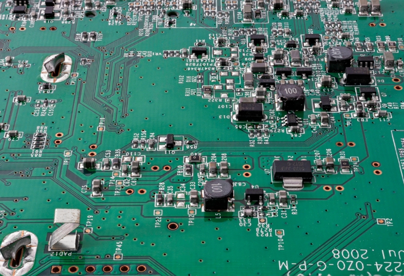
Package Case
Chip 3D Stacking
Packaging Case
Nuclear Industry
Reliability Products
Packaging Case
High-Power Laser
Packaging Case
Infrared Chip
Packaging Case
Atomic Clock
Packaging Case
Packaging Case


Main application scenarios
Main application scenarios
Why choose us
With the business tenet of "being down-to-earth and honest", the company provides customers with high-quality products with reliable quality, economical price, simple use, energy conservation and consumption reduction
Torch is a professional electronic assembly equipment and service provider, is engaged in SMT production equipment and consumables research and development, production, sales of high-tech enterprises
Years of technical accumulation and profound strength
01
BRAND STRENGTH
Under the guidance of the spirit of "working together to build a city", "technology standing, industry serving the country" and corporate culture, all comrades of the company are working hard to promote the automation, industrialization and scale of China's electronic industry
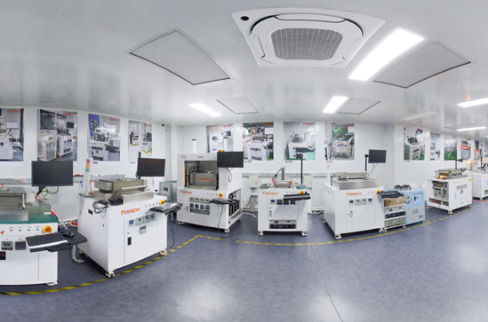
The company has developed and produced dozens of professional SMT production, testing equipment and scientific research equipment, such as large and medium-sized lead-free series reflow soldering, wave soldering, semi-automatic screen printing machine, patch machine, etc
Advanced technology and independent research
02
INNOVATION ABILITY
With the business tenet of "being down-to-earth and honest", the company provides customers with high-quality products with reliable quality, economical price, simple use, energy conservation and consumption reduction
Torch is a professional electronic assembly equipment and service provider, is engaged in SMT production equipment and consumables research and development, production, sales of high-tech enterprises
Years of technical accumulation and profound strength
03
PRODUCT QUALITY
About us
Brand Profile
Honor
corporate culture
Video materials
organization
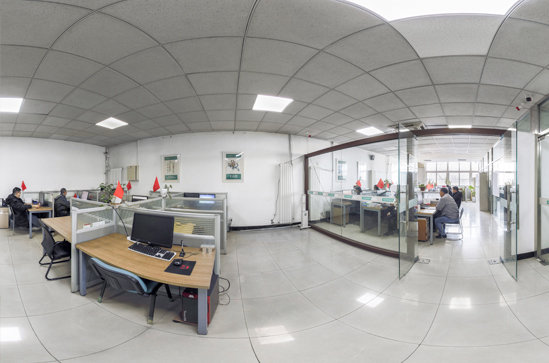
Torch Technology was founded on October 12, 2005, the company is located in Beijing, the capital of China, the legal representative is Zhao Yongxian. Is a professional electronic assembly equipment and service provider, is engaged in SMT production equipment and consumables R & D, production, sales of high-tech enterprises, currently has a number of molecular companies. Our company completed shareholding transformation on November 5, 2015. In the process of providing professional SMT services for domestic and foreign electronic manufacturers for a long time, Comrade Technology
TORCH Semiconductor (Jiangsu) Co., Ltd
Company strength


News information


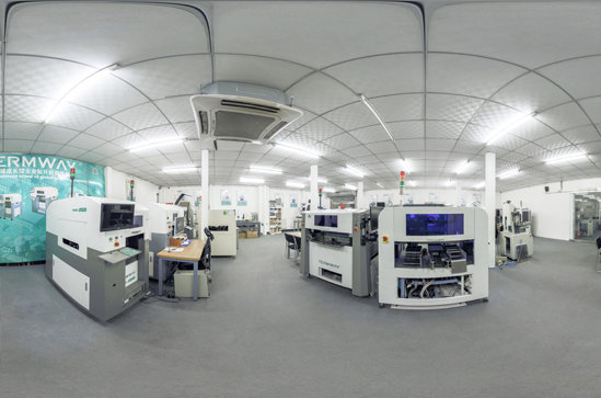
Cooperative brand


Copyright © TORCH Semiconductor (Jiangsu) Co., Ltd
Tel:400-998-9522
Email :sales@torch.cc
North factory address :No.15, Jingsheng South 4th Street, Central District, U Valley Science Park, Liandong District, Tongzhou District, Beijing
Address of South Factory:No. 18, Kechuang Road, High tech Industrial Development Zone, Taixing City, Jiangsu Province

WeChat consulting

Follow us
Follow us
Tel
Contact us
 Online Service